

The assembled board should be tested and inspected for performance. Manual checks: A visual inspection done in individual by a designer to make sure the quality of a PCB. Automatic optical inspection: An inspection technique more applicable for bigger batches of PCBAs. An automated optical inspection machine, or AOI machine, makes use of high-powered cameras, set at totally different angles to view the solder connections. A plated by means of-hole, or PTH, element is a gap within the PCB that’s plated by way of the board. Rather than soldering paste, more specialised soldering technique is required for PTHs. Manual soldering: A manual, by-hole insertion. Wave soldering: The automated model on manual soldering where a wave of molten solders all of the holes in the underside of the board at once. Note: A solder paste applier, choose-and-place machine, excessive-pace chip shooter, and infrared oven inserted in a conveyor configuration can apply solder, decide-and-place, and solder 50,000 parts or extra in an hour. Once the soldering strategy of the PCB board meeting is full, it is time to do a ultimate inspection and useful take a look at. Run energy and simulated indicators to test the PCBs electrical traits. A sign that the PCB has failed is when it exhibits the fluctuation of electrical alerts in the course of the take a look at. If the PCB fails the final inspection, it must be scrapped. And pcba the method begins throughout till a profitable PCB is produced.
The method by which the naked printed circuit boards, PCBs utilized in digital products is evey bit as essential as the assembling with components. PCB manufacture basics How to choose the proper PCB producer The PCB manufacturing course of is very important for anyone concerned in the electronics business. Printed circuit boards, PCBs, are very broadly used as the idea for electronic circuits. Printed circuit boards are used to supply the mechanical foundation on which the circuit could be constructed. Accordingly just about all circuits use printed circuit boards and they’re designed and used in portions of millions. Although PCBs form the basis of nearly all electronic circuits in the present day, they are typically taken without any consideration. Nevertheless know-how in this area of electronics is moving forward. Track sizes are reducing, the numbers of layers within the boards is growing to accommodate for the elevated connectivity required, and the design rules are being improved to ensure that smaller SMT devices might be handled and the soldering processes used in production may be accommodated.
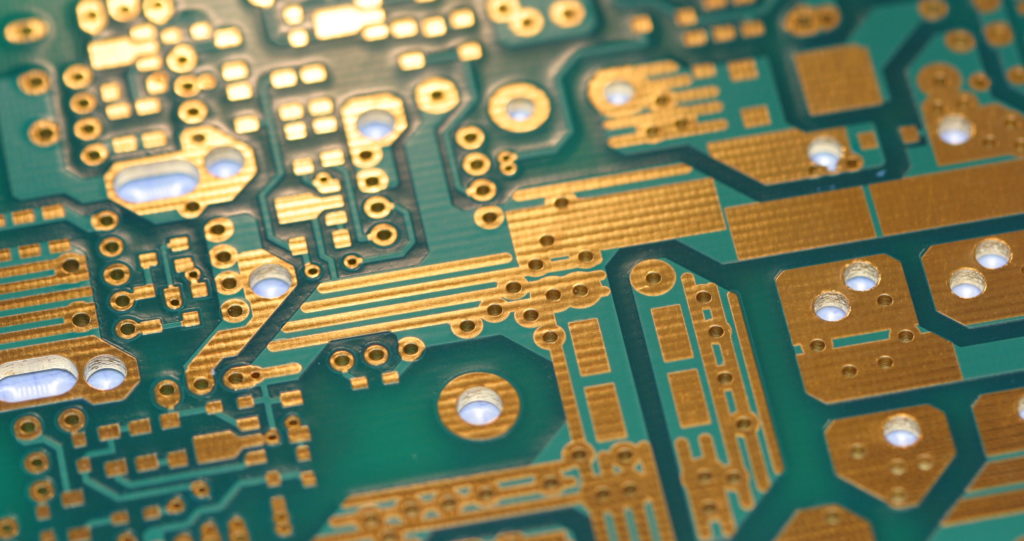
 The PCB manufacturing process could be achieved in a selection of the way and there are plenty of variants. Despite the many small variations, the main levels in the PCB manufacturing process are the identical. Printed circuit boards, printed circuit board PCBs, will be made from a variety of substances. The most widely utilized in a type of glass fibre based mostly board known as FR4. This provides an inexpensive diploma of stability beneath temperature variation and is doesn’t breakdown badly, whereas not being excessively costly. Other cheaper materials can be found for the PCBs in low cost industrial merchandise. For high efficiency radio frequency designs where the dielectric constant of the substrate is vital, and low levels of loss are wanted, then PTFE primarily based printed circuit boards can be used, though they’re far harder to work with. In order to make a PCB with tracks for the components, copper clad board is first obtained. This consists of the substrate material, typically FR4, with copper cladding usually on both sides.